main
To the list of lectures
|
§3 Intrinsic conductivity of semiconductors
A considerable quantity of substances which occupy on the electrical properties the intermediate standing between conductors and dielectrics concerns semiconductors. For semiconductors (j = 1 2¸10-8 S/m; j - specific electroconductivity). For j =1 4÷103 S/m conductors; for dielectrics j < 10-12 S/m. The major property and a sign of semiconductors is dependence of their electrical properties on exterior conditions Т, Е, р etc. Prominent feature of semiconductors consists in reduction of their specific resistance with temperature magnification. For semiconductors the crystalline structure with a covalent binding between atoms is characteristic.
Under the influence of exterior factors some valence electrons of atoms gets energy, sufficient for voiding of covalent bindings.
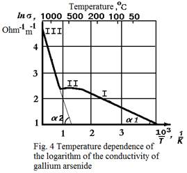
The exit from an electron covalent binding on the energy diagramme corresponds to transition from a valence band in a conduction band. At voiding of an electron from a covalent binding in last there is as though an empty seat possessing the elemental plus charge, equal on absolute value quantity to an electron charge. Such place released in an electron coupling have conventionally termed as an electron hole, and process of formation of pair has gained the name generation of charges. An electron hole, possessing are plus a charge, associates to itself an electron of the next filled covalent binding. As a result of it one communication (this process is termed as a recombination) is reestablished and the next collapses. Then it is possible to speak about travel of the plus charge - electron holes on a crystal. If on a crystal the electric field operates, the motion of electrons and electron holes becomes ranked and in a crystal there is an electric current. Thus a hole conductivity term as conductivity of p-type (positive - plus), and electronic conductivity of n-type (negative - minus). In chemically pure crystal the semiconductor (number of impurities 1016 м-3), number of electron defects to always equally number of free electrons and the electric current in it is formed as a result of simultaneous transport of a charge of both signs. Such electron-hole conductivity is termed as natural conductivity of the semiconductor. j = jn + jp j - density of a current of electrons (n) and electron holes () In the intrinsic semiconductor the Fermi level is in the forbidden band middle. As the activation energy equal to breadth of a forbidden band goes on transfer of an electron from valence band top level on the inferior level of a conduction band and simultaneously on electron hole occurrence in a valence band. I.e. the energy spent for formation pair of carriers of current is divided on two equal parts, and thus a reference mark for each of these processes (transition of an electron to an electron hole birth) should is in the forbidden band middle. Quantity of the electrons which have transferred in a conduction band and quantity of formed electron holes ~ N(e) » eΔE/2kT Thus specific conductance of corresponding semiconductors j = j e–ΔE/2kT j - a stationary value spotting a view of substance. I.e. with magnification Т it is incremented j, as from the point of view of a band theory the number of electrons which in a consequence of thermal excitation transfer in a conduction band increases. lnj = lnj –ΔE/2kT. I.e. lnj~1/T On a line declination of lnj it is possible to spot forbidden band bread th DE.
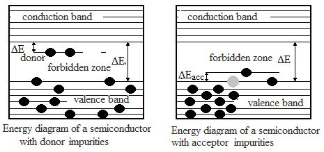
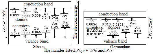
§4 An impurity conductivity of semiconductors.
In the semiconductors containing an impurity, electroconductivity be made up from intrinsic and the impurity. The conductivity caused by presence at a crystal of the semiconductor of impurities from atoms with other valence is termed as the impurity. The impurities causing in the semiconductor magnification of free electrons, are termed donor, and causing magnification of electron holes - acceptor.
Various activity of the impurity atoms speaks as follows. We will guess that in a germanium crystal (Ge4+) which atoms have 4 valence electrons, we will enter the five-valence arsenic As5+. In this case atoms of arsenic the 4th of five valence electrons take up. 5th valence electron of arsenic will appear not related, i.e. there is free the electromagnetic semiconductor which electroconductivity has raised thanks to formation of surplus of free electrons at impurity introduction are termed semiconductors with electrical conductance (electron semiconductor), and an impurity donor (donating an electron).
Energy levels of donor impurities are termed as donor levels - located under the inferior level of a conduction band.
At semiconductors p-type at Т = 0 K, in the middle between an acceptor level and a valence band ceiling. With increase Т ЕF it is biased to the middle of a displaced band. Dependence of conductivity of semiconductors on temperature looks like, shown in figure (look laboratory operation 8.6 more in detail.). |